The part nobody asks about — until the line width won't hit spec
If you ask most people in electronics manufacturing what determines PCB yield, you'll hear about etch chemistry, exposure equipment, copper foil quality, maybe the cleanroom itself. Almost nobody says "the nozzle." And for years, that was a fair answer — tolerances were loose enough that a decent, generic spray nozzle got the job done.
That's no longer true. As chip packaging moves deeper into the AI era, the line-width tolerance that etching has to hit has been shrinking steadily — from a traditional ±10%, down to roughly ±6% for AI-era substrates, and now, on some of the most advanced programs, as tight as ±5%. At that point, the nozzle stops being a background part and becomes one of the things that actually decides whether a panel passes or fails.
This article walks through why that is, in plain terms first, then in the level of detail our process engineers actually work in. If you're a purchasing manager, plant manager, or engineer new to wet processing, the first few sections will get you fully oriented — and if you want the fundamentals first, LORRIC's overview of PCB types and the manufacturing process is a good starting point before coming back here. If you're already deep in DES process work, stick around for the customization logic further down — that's where the real yield gains tend to hide.
Start with the basics: what is the DES process actually doing?
 The three DES stages share one upstream dependency: how evenly chemistry lands on the board. This cycle runs at both the inner-layer and outer-layer imaging stages of real PCB fabrication.
Here's the part that matters for this article: all three of those stages depend on one upstream thing — how evenly the chemistry actually lands on the board. That gives you a simple chain:
Nozzle uniformity → chemical distribution → etch uniformity → line-width Cpk → yield.
Worth noting: real PCB fabrication runs this DES cycle more than once — typically at both the inner-layer imaging stage and again at the outer-layer imaging stage. The nozzle logic below applies identically each time it runs, which is exactly why getting it right matters twice as much as it might first appear.
Think of it like a garden sprinkler system. If the sprinkler heads spray unevenly, some patches of your lawn get soaked and others stay dry — no amount of fertilizer fixes that, because the problem is upstream of the fertilizer. Etch chemistry works the same way. If the nozzle's spray pattern is uneven, you can have perfect chemistry and a perfectly calibrated line, and you'll still get uneven etching, because the unevenness was baked in before the chemistry ever touched the board.
Why PCB line-width tolerance keeps getting tighter in the AI era
For most of PCB manufacturing's history, line-width tolerance sat around ±10% — on a 100 μm line, that's a working window of roughly 90 to 110 μm. That's a comfortable margin. It absorbs small variations in equipment, chemistry, and yes, nozzle performance, without anyone needing to think too hard about the nozzle specifically.
AI-driven substrates changed the math. As AI accelerators, GPUs, and HPC processors pack more layers and finer routing into their substrates, the industry baseline has tightened to roughly ±6% — 94 to 106 μm on that same 100 μm line. And now, among the customers building the most advanced AI/HPC packages, we're seeing requirements pushed further still, down toward ±5% — essentially half the margin that traditional PCB processes were designed around.
This isn't a one-time adjustment the industry will settle into. Analysts tracking AI substrate demand describe a multi-year structural shift, with substrate layer counts and package areas expanding sharply as AI chips scale up — and that expansion is straining not just materials supply, but the entire fine-line patterning process window.[1][2] Independent analysis of AI/HPC substrate manufacturing points to fine-line patterning accuracy as one of the primary yield bottlenecks in these builds, because at this scale, even a small defect in line formation eats a disproportionate share of total panel yield.[3]
For a nozzle, this matters in a very specific way. Halving your tolerance window doesn't mean "spray a little more carefully." It means things that used to be invisible — small inconsistencies in the nozzle's own manufacturing tolerance, minor drift in spray angle, a slightly uneven distribution profile — stop being invisible. They become the reason a line can't hit Cpk, even when everything else about the process is correct.
"Just get a better nozzle" is the wrong instinct
Here's a mistake we see constantly, and it's an understandable one: assuming that tighter tolerance requirements mean you should buy a more expensive, higher-grade nozzle. In reality, nozzle selection for DES is a matching problem, not a price-tier problem. The right nozzle is the one engineered for your specific combination of equipment, board, chemistry, and line speed — and that's rarely the same answer twice.
A couple of examples make this concrete.
Copper thickness changes what you need from flow rate. Heavy copper needs a higher flow rate and stronger impact force, because you need enough force to keep replacing chemistry deep in the features as etching proceeds. Thin copper needs the opposite — a lower flow, more delicate impact — because too much force just over-etches it. A nozzle that's great for one will actively work against you on the other.
Heavy copper
 Higher flow, stronger impact force
Thin copper
 Lower flow, more delicate impact
Where the nozzle sits — above or below the board — changes the physics. Top-mounted spray has to deal with a pooling effect on the board surface that slows chemical replacement, and with back-splash risk when spray hits conveyor rollers. Bottom-mounted spray avoids that pooling and lets chemistry recirculate more efficiently, but now the impact angle has to be adjusted for the board sagging slightly under its own weight as it travels. These aren't two versions of the same problem — they're genuinely different engineering problems that call for different nozzle configurations.
Top and bottom spray aren't two versions of the same setup — they're different engineering problems, each with its own tradeoffs.
There's a third layer to this that's easy to miss: the board doesn't behave the same way at every point along its length. As a panel moves through the line, the leading edge is still wetting out and just beginning to react, the center reaches a steady etch rate, and the trailing edge can accumulate chemistry — which risks over-etching or unevenness if nothing adjusts for it. Getting a uniform result across the whole board means adjusting nozzle height, angle, and pitch together along that length, not setting one configuration and assuming it holds everywhere.
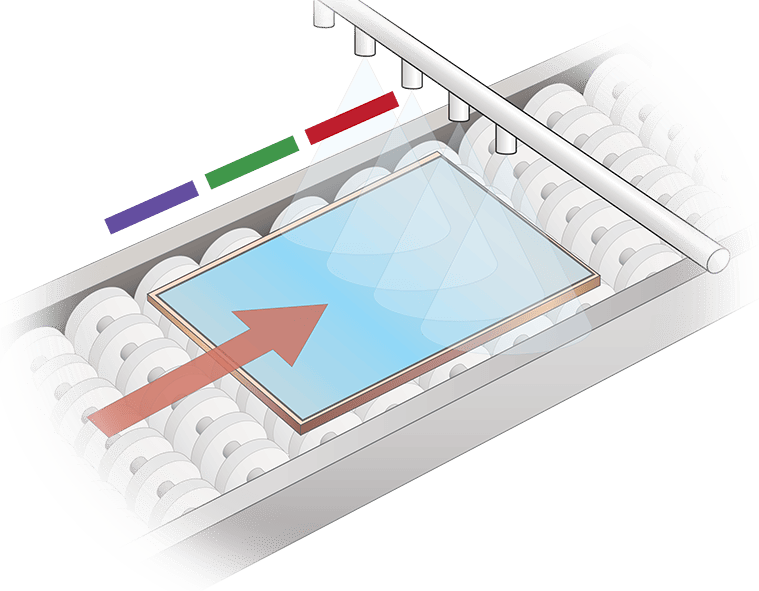
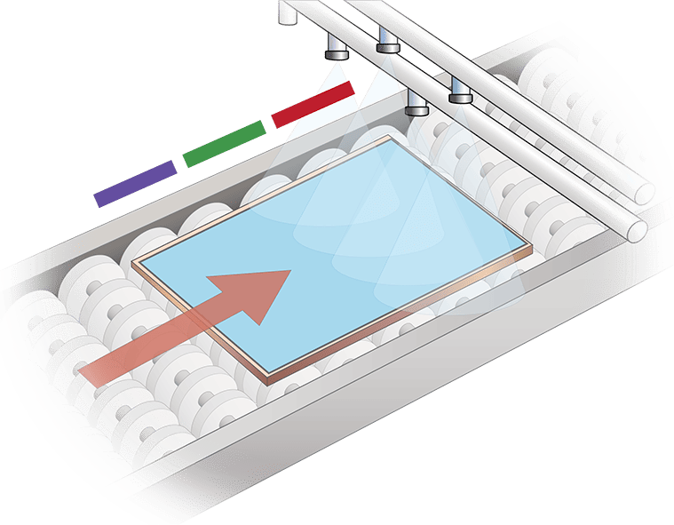
Same nozzle setup everywhere leaves the resulting spray/etch uniformity uneven across the board's length. Tuning height, angle, and pitch per zone keeps it consistent from leading edge to trailing edge.
Flat fan or cone? Why the industry is leaning one direction
Flat fan nozzles have served general cleaning and standard etch work well for a long time — they produce a clean, linear spray footprint, and they're a sensible default when tolerances are loose. Their weak point shows up specifically as tolerances tighten: flat fan patterns tend to etch slightly differently along horizontal traces than vertical ones. At ±10%, that difference is background noise. At ±5%, it can be the difference between passing and failing Cpk.
Cone nozzles spray a radially uniform footprint with much less of that horizontal/vertical bias, which is why they've become the default choice on AI-era lines where the tolerance window leaves no room to absorb directional variation. This is a good example of something that used to be a "nice to have" quietly becoming a hard requirement as the industry's specs tightened around it. (LORRIC's own KD/KDMF two-piece cone nozzle line was built specifically for PCB etch and develop applications, if you want to see what this looks like as an actual part rather than a concept.)
Flat Fan Nozzle
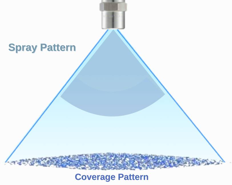
Width changes with direction
Full Cone Nozzle
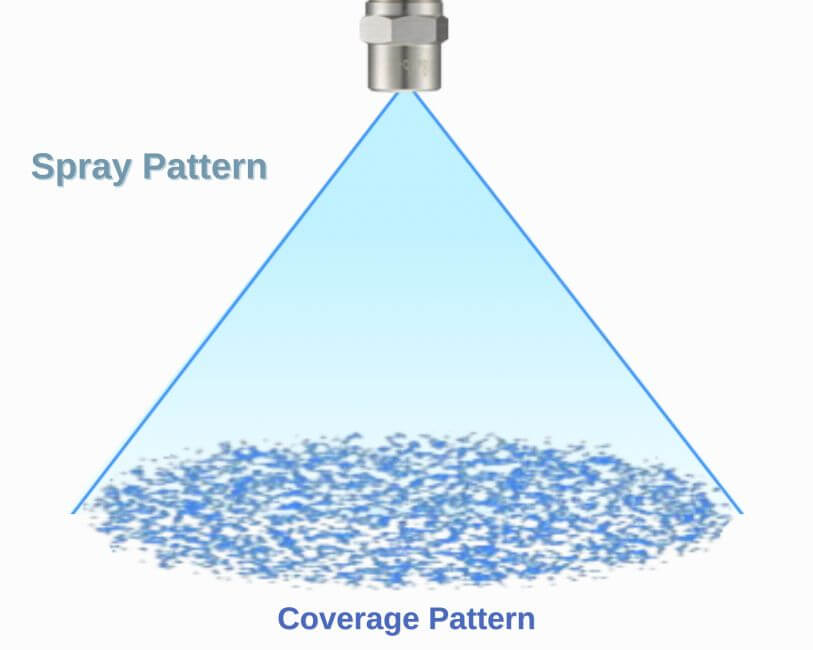
Width same in every direction
Not all cone nozzles are actually uniform
Switching to a cone nozzle doesn't automatically solve the problem, though — and this is a detail that's easy to overlook until you look closely at the spray face itself. A lot of cone nozzles on the market aren't as uniform as their shape suggests. Up close, many show a handful of concentrated streams rather than a smooth, even distribution, simply because of how the internal flow channels are designed.
A well-engineered multi-channel cone nozzle addresses this directly, by shaping the internal flow paths so chemistry distributes evenly across the entire spray face instead of concentrating into a few dominant jets. It's the difference between a nozzle that's a cone nozzle by shape and one that actually delivers cone-nozzle uniformity in practice — a difference that's genuinely hard to see at loose tolerances and impossible to ignore at tight ones.
Competitor cone — concentrated streams
 A few dominant jets, uneven coverage
LORRIC multi-channel — optimized
 Evenly distributed across the full spray face
What this looks like when it actually happens on a line
We've seen this play out on a real advanced-substrate line: tightening line-width requirements started causing a Cpk shortfall, showing up as localized line-width shift, a noticeable gap between edge and center Cpk, and a measurable difference between horizontal and vertical line behavior.
The fix wasn't a part swap. It was a re-engineering of the nozzle system as a whole:
- Moving to a multi-channel cone nozzle design
- Re-sizing flow rate based on the actual copper thickness in use
- Recalculating nozzle height, angle, and pitch together, rather than adjusting one variable at a time
- Configuring the top and bottom nozzles differently instead of assuming a symmetric setup would work
The result was better spatial uniformity, Cpk moving from insufficient to acceptable, a smaller horizontal/vertical gap, and improved yield on the fine-line product. The exact numbers from that case are under customer confidentiality, so we won't publish them here — but the pattern is the repeatable part: a systems-level look at the nozzle, not a single-component substitution.
For a concrete, named example of this same logic in practice — including the quick-release nozzle design and the measured yield result — see LORRIC's case study, Quick-Release Nozzles × PCB DES: Better Spray, Higher Yield. (Note: the ±5% figure in that case study refers to the QFMF nozzle's own flow/angle manufacturing tolerance — a different number from the customer line-width tolerance discussed above, even though they share the same figure.)
The takeaway
As tolerances move from ±10% toward ±6%, and toward ±5% on the most demanding AI/HPC programs, the margin for nozzle-driven error is shrinking faster than most plants' nozzle specs have kept up with. Getting this right means treating nozzle selection as a customization exercise — copper thickness, spray direction, position along the board, and internal flow-channel design, considered together — rather than a catalog pick. Fabs that keep treating nozzles as an interchangeable commodity often find, eventually, that the nozzle — not the chemistry, not the equipment — is quietly the thing capping their Cpk.
Frequently Asked Questions (FAQ)
What is Cpk in PCB manufacturing?
Cpk is a process capability index — a standard statistical measure of how consistently a manufacturing process stays within its required tolerance window, not just on average but accounting for variation. In PCB etching, Cpk is what actually gets measured to confirm a line hits its line-width spec; everything this article discusses — nozzle uniformity, tolerance tightening, customization — ultimately shows up as a change in Cpk, for better or worse.
How tight are line-width tolerances getting in AI-era manufacturing?
Traditional PCB work has generally run around ±10%. AI-era substrate processes have tightened that to roughly ±6%, and some of the most advanced AI/HPC programs are now specifying tolerances as tight as ±5%.
Is a cone nozzle always the right choice over a flat fan?
Not automatically — it depends on the process. Cone nozzles generally handle horizontal/vertical uniformity better, which matters more as tolerances tighten, but the right choice still depends on matching the nozzle to copper thickness, spray orientation, and the specific equipment, not on nozzle type alone.
Will a more expensive nozzle fix a yield problem on its own?
Usually not, and this is one of the most common misconceptions we run into. Nozzle performance comes from matching flow rate, geometry, height/angle/pitch, and internal channel design to the actual line — a higher-priced nozzle that isn't configured correctly for those conditions won't reliably outperform a well-specified, lower-cost one.
References
- AI chip demand tightens ABF substrate supply — Digitimes, 2026. digitimes.com
- Glass substrates and AI chip packaging bottlenecks — TrendForce Insights, 2026. insights.trendforce.com
- IC Substrates for AI and High-Performance Computing: Design and Material Considerations — JHYPCB. pcbelec.com